In the ever developing sector of electronics where various brands bring their concepts to life, the technology of PCB assembly is pivotal. With the advancement in levels of technology, several calls have been made for improved, faster and more flexible methods of assembling PCB. Therefore, this blog covers the present status of PCB assembly, the issues and opportunities it faces and trends that define its progress. Thus, outlining the above trends, electronics manufacturers are sure to discover that they are preparing for shifts in approaches to hardware creation.
What is PCB assembly?
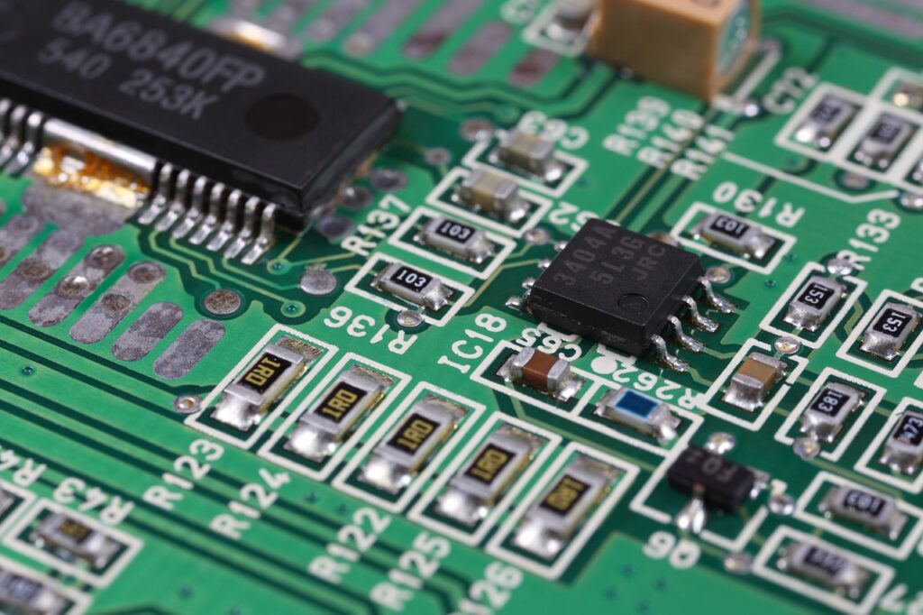
- The most asked question is what is PCB assembly? The answer is,Printed Circuit Board assembly commonly referred to as PCB assembly involves placing and mechanically affixing Electronic components onto an electrical circuit set on a PCB.
- It is a process that has several sub-processes among them are placement of the components, soldering, visual inspection and testing.
- The assembly can operate on a single line where it is done by hand or there can exist automated systems where it is done based on the type and number of products to manufacture.
Traditional PCB Assembly Methods
- Through-hole technology: Parts which need to be connected to the board are mounted through holes made in the board and soldered at the back.
- Surface-mount technology (SMT): Components are hand placed directly onto the surface of the board and soldered on the board.
- Mixed technology: A product in which a part of the components is插Styled through holes while the other part is mounted on the surface of the board.
Issues that exist in Conventional Surface Mount and Through Hole Assembly
- Longer cycle since it is not appropriate for short-run production and usually used where prototypes are created.
- High fixed costs on the assembly lines used in automating these products.
- Low tolerance for modifications in the design/prototyping cycle.
- Sluggishness when it’s necessary to either increase or decrease the rate of production.
The Rise of Automated PCB Assembly
- Pick-and-place machines: Pace and precision with which parts are placed on board:
- Reflow ovens: Tin is used to join the components to the board by melting the solder paste at required joints.
- Automated optical inspection (AOI) systems: Find flaws and control the quality of the produced goods.
These systems have gone a long way in enhancing the speed of production and at the same time boosting the level of accuracy.
Software-Driven Manufacturing in PCB Assembly
- Design software and its connection to assembly operation.
- Digital twin technology: Instantiation of real physical PCBs for purposes of test and optimization using virtual electronic means.
- Dynamic control of assembly parameters in relation to the progress of the task.
- Frees up the design process for quicker models and better production time.
Advancements in Component Placement
- Heavy-Duty Placement machines that can place thousands of components in a single hour.
- Specific guided vision systems for extremely accurate positioning of the components.
- As feeders they should be versatile in the sense that they should adapt to the characteristics of a number of different components and their sizes.
Innovations in Soldering Techniques
- Selective soldering: Soldering involves proper application of solder, on certain parts of the printed circuit board.
- Laser soldering: Special soldering of very sensitive fine pieces of the circuit board.
- Vapour phase soldering: For additional information, one must note that most standardised heaters offer equal heating for the multi-layer and structure board.
Consolidated Improvement of Quality Control and Testing
- 3D solder paste inspection: It guarantees that a solder paste is rightly applied on the PCB before the components are placed.
- X-ray inspection: Hearths embedded defects on Multi-Layer Board and Ball Grid Array (BGA) parts.
- In-circuit testing (ICT) and functional testing: Check proper connection of wires and other electrical aspects.
Miniaturization and High Density Interconnect also called as HDI Boards
- The consumers of the small and intricate PCBs in user electronics goods.
- HDI technology principals make it possible to pack more components and or have finer circuit traces.
- Difficulties in assembly because of the fact that the component sizes are smaller and tolerances are very strict.
Flexible and Rigid-Flex PCBs
- Increased adoption in applications that require compact size and integration into the human body.
- Has assembly requirements and tools that are not common and easy to practise in most of the factories.
- Permits new Electronic solutions and design features.
Environmental Considerations in PCB Assembly
- Use of costly lead-free solders to meet the requirements of the Restriction of Hazardous Substances directive.
- Energy efficient processes are followed for the assembly of a product.
- A shift towards the use of recyclable and more environmentally friendly materials.
The Role of Artificial Intelligence in PCB Assembly
- Defect detection and classification systems inbuilt with the help of Artificial Intelligence.
- Preventive services for assembly equipment.
- The areas encompass the improvement of component placement and routing algorithms.
Industry 4. 0 and Smart Factories
- Implementation of Internet of Things to detect and control the execution of assembly processes in real time.
- Data analytics for the enhancement of the processes and reducing the variability systematically.
- Greater usage of machinery and minimum intervention of people in certain types of assembly.
Challenges in Modern PCB Assembly
- Adapting to the fast changing component technologies.
- Coordinating the issues of product variety, flow and operating characteristics of high mix / low volume manufacturing.
- The dilemma of choosing between affordable prices for the equipment and higher quality.
- Granting focus for bridging the skills gap in the workforce especially as technology takes over diverse aspects of our lives.
The future of PCB assembly
- Larger incorporation of addendum manufacturing processes.
- Recent innovations in the electronic industry have seen poor self-assembly of components attached to the surface.
- Use of nanomaterials together with nanoelectronics in the production process of PCBs.
- Higher volume of modular and adaptable assembly line systems.
Conclusion
The evolution of PCB assembly is rising continuously, through the changes of technology such as automation as well as the integration of software technology. Very much dependent on the industry of electronics, but PCB assembly processes are gradually shifting to be far more versatile, fast and integrated with software engineering paradigms. Through these changes and pro-active technology investments, electronics manufacturers can thus continue to optimise this production chain, and manage to launch the next-generation electronic products into the market faster in response to rapidly emerging and evolving demand for more and newer forms of electronics.
Success in the industry therefore depends on the ability to integrate hardware and software development especially in the assembly of the PCBs, as it is likely to lead to product development cycles that are more innovative and efficient in the future.